
Products
Products Category
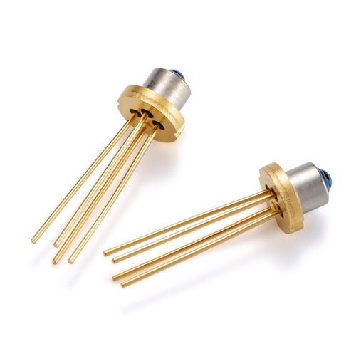
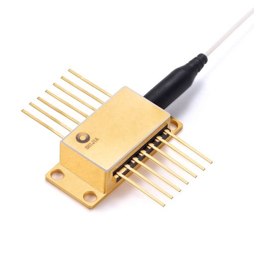
Optical Active Lasers Platform
.jpg)
.jpg)
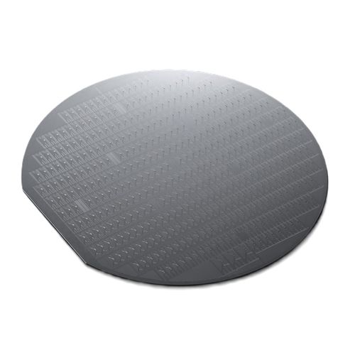
*Possesses fully independent epitaxial development and production capabilities
*Equipped with dual-material technology involving InGaAsP and AlInGaAs
*Mature epitaxial structure reserve covering the full wavelength range of 1260~1700nm
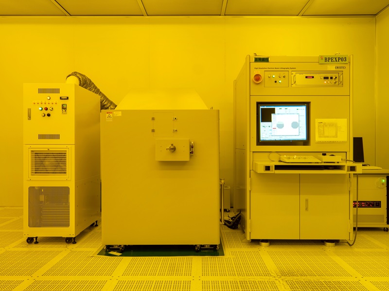
*Ultraviolet exposure technology *Fully automatic photoresist coating and development system
*Sub-nanometer electron beam lithography technology *Phase grating technology
Maximum Growth Thickness: 10 micrometers Thickness Uniformity: ±2% Refractive Index Uniformity: ±0.0003
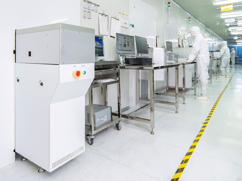
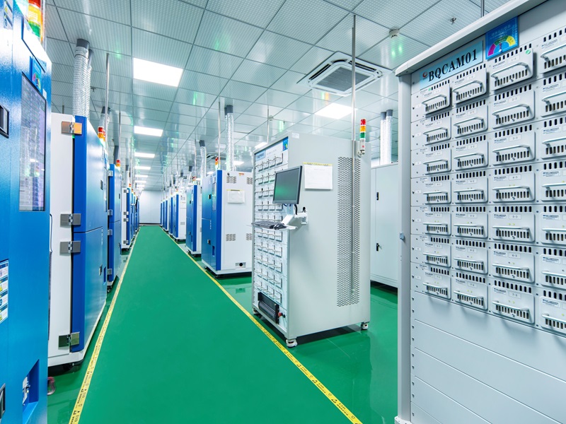
*Accumulated years of wafer process detail experience
*End-to-end informationized production control with manufacturing execution system(MES)
*Automated chemical etching, cleaning, and other process workflows *Exclusively designed non-contact fixtures for P-side handling
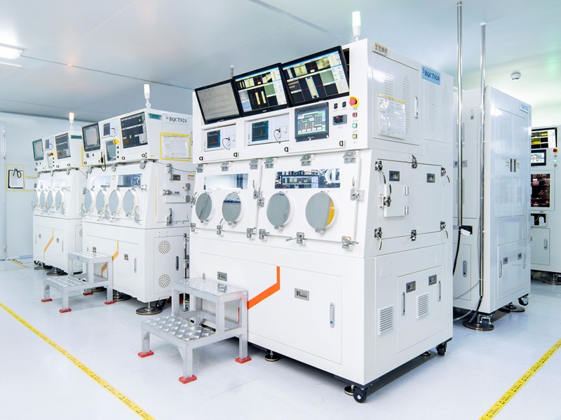
*Fully automated chip testing and grading capabilities
*Chip-level product testing capability at operating temperatures ranging from -40°C to 95°C
*Ability to test and analyze important optoelectronic parameters such as optical power, spectrum, backlight, far-field divergence angle, etc.
*Chip-level reliability verification, individual assessment for each wafer, ensuring precise quality control
*Airtight and non-airtight aging tests, high-temperature aging tests, dual 85 tests, low-temperature storage, temperature cycling tests, ESD (Electrostatic Discharge) tests, push-pull force tests
*High-speed Chip-on-Carrier (COC) packaging & TO packaging, temperature-controlled & high-power TOSA (Transmitter Optical Subassembly), and other specialized device packaging design capabilities
*High-speed optical eye diagram and optical fiber sensitivity testing system
*Bandwidth testing system
*Relative Intensity Noise(RIN) testing system
*Linewidth testing system
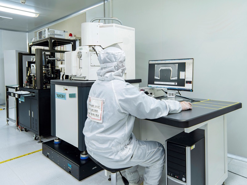
*50,000x magnification process monitoring *Intuitive observation of the process development progress